An SPDT solid state relay switches electronically between two paths without moving contacts. Implementation methods include integrated Form C devices, paired normally open and normally closed outputs, or two normally open SSRs coordinated by an external controller.
Each approach must maintain the necessary connection states throughout operation, particularly when replacing an electromechanical changeover relay.
What Is an SPDT Solid State Relay?
An SPDT solid state relay performs a single-pole, double-throw switching function using semiconductor outputs. A common circuit node routes through one conduction path or the other.
Solid-state switching paths follow standard contact forms:
- Form A defines a normally open path that conducts under active control.
- Form B defines a normally closed path that conducts without input drive.
- Form C defines a changeover function between normally open and normally closed paths.
A solid-state Form C device may provide separate output pairs that require external wiring to establish the common node. The pin diagram defines the required layout. Two independent outputs do not inherently deliver changeover functionality. Complementary steady-state signals can still produce overlapping conduction during switching transitions.
SPDT Solid State Relay Circuit Options
Path selection with solid state relays generally relies on three configurations, each requiring different levels of control logic and external circuit coordination.
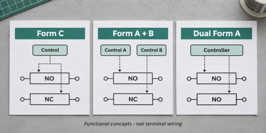
Integrated Form C SSRs
Integrated Form C SSRs combine normally open and normally closed paths under a single control input. They suit signal routing within rated voltage, current, and on-resistance limits. Confirm whether the common terminal is connected internally or requires external wiring across output pins. Form C ratings do not guarantee break-before-make switching; verify explicit timing specifications to prevent cross-conduction.
Form A and Form B Combinations
Pairing Form A (NO) and Form B (NC) channels provides complementary outputs from discrete devices or shared packages. While steady states remain opposite, propagation delay mismatches can cause brief cross-conduction. This layout provides a passive normally closed path, but the surrounding circuit must manage switching overlap. Tying control inputs together does not eliminate transition timing skew.
Dual Form A SSR Circuits
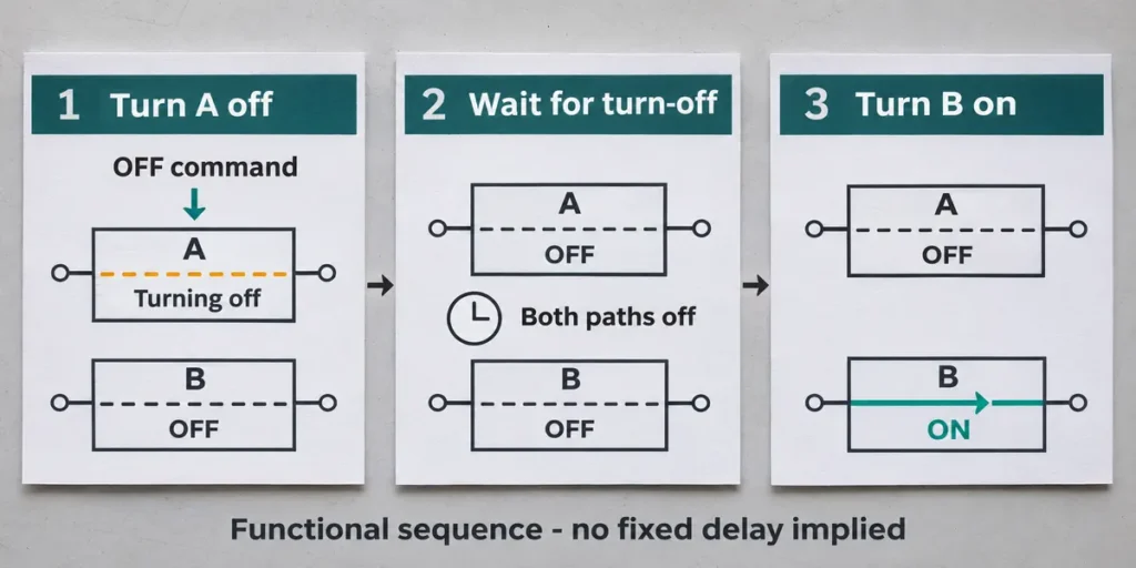
Dual Form A circuits use two independent normally open outputs. For single-source DC routing with bidirectional MOSFETs, connect one terminal of each channel to supply node C and the remaining terminals to loads A and B, verifying pinouts before bridging. Switching loads requires turning off the active channel, waiting for full turn-off, and then enabling the second path.
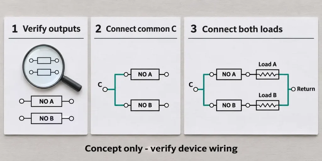
For AC loads, a dual-channel AC SSR houses two switches in one package but lacks internal interlocks, cross-wiring, or complementary logic. This layout suits systems that tolerate an all-off state during power loss, but it cannot provide a passive normally closed path.
When Can a Dual-Channel SSR Replace an SPDT Relay?
A dual-channel SSR can substitute for an SPDT mechanical relay if the circuit accommodates its wiring topology, transition timing, and de-energized output states.
Two circuit roles must be distinguished: alternating power between isolated loads versus routing a single node between two paths. Shared-node routing requires compatible output configurations. Do not tie output terminals together without verifying internal semiconductor structures and channel-to-channel isolation.
Operating conditions below reflect intact devices with load voltage present and input drive removed. The mechanical comparison assumes a non-latching relay.
| Solution | Output Topology | Control Method | Control-Off Behavior | Main Limitation |
| Integrated Form C SSR | NO and NC paths; common connection follows pin diagram | Shared input | NO blocks; NC conducts after settling | Transfer timing needs explicit verification |
| Form A + Form B combination | Separate NO and NC output pairs | Coordinated input drive | A blocks; B conducts after settling | Switching delays can cause overlap |
| Dual Form A SSR circuit | Two NO paths with suitable external connections | Separate commands with interlocking | Both block after turn-off completes | No passive NC path |
| Mechanical SPDT relay | Shared moving contact with NO and NC terminals | Coil drive | Common returns to NC | Contact wear, bounce, and finite switching life |
Functional interchangeability does not make these drop-in replacements. Differences in pin layouts, drive currents, off-state leakage, and conduction losses frequently demand circuit adjustments.
How to Choose the Right SPDT SSR Solution
Integrated Form C devices address signal switching when ratings match. Independently controlled Form A channels suit applications that tolerate an open-circuit state without power and have external timing control.
Load Requirements
Signal circuits require checking on-resistance, off-state leakage, and output capacitance. High resistance drops signal voltage, while capacitance couples high-frequency signals across an open path.
Power loads require verifying AC or DC supply, continuous current, inrush surges, and polarity. TRIAC and SCR outputs switch erratically if load current or voltage falls below specified holding thresholds. Thyristors suit AC loads; DC circuits require transistor or MOSFET outputs capable of breaking direct current. Connection steps are detailed in the SSR wiring guide.
Startup and Power-Loss States
Switching states must be defined for power-up routines, controller resets, input signal dropouts, and auxiliary supply failures. A controller actively driving an off-state behaves differently from an unpowered unit with floating I/O pins. Two Form A outputs cannot maintain a conductive path without control power. While a Form B output provides a normally closed path, its conduct state must be evaluated against the actual supply architecture. Unpowered default states do not protect against unexpected hardware faults.
Switching Timing and Interlocking
Break-before-make operation prevents shorting power rails or running conflicting loads. Software interlocks block concurrent turn-on commands, while dead time separates channel transitions. Timing budgets must account for maximum turn-off delays, controller latency, and temperature drift. AC thyristors do not open immediately upon control removal; conduction persists until current drops below the holding threshold near an AC zero crossing. Conduction onset also depends on zero-cross and random turn-on behavior.
Electrical and Thermal Ratings
Output voltage ratings must withstand peak blocking potentials and line transients; evaluate peak values rather than RMS. Current limits must reflect thermal derating for actual ambient temperatures rather than absolute stress limits. MOSFET conduction losses scale with current squared multiplied by operating-temperature on-resistance. Shared packages also impose total dissipation limits. High-power modules require heat sinks and suitable mounting conditions. Verify input drive limits, input-to-output isolation, and channel-to-channel isolation.

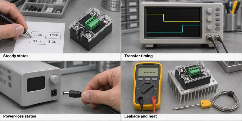
Circuit Validation
Testing the assembled circuit under representative load conditions requires verifying:
- The intended steady-state connections.
- Output overlap and interruption time in both directions.
- Startup, reset, and control-power removal.
- Off-state load behavior and temperatures during sustained operation.
Oscilloscope measurements capture transition timing under bench conditions. Bench tests at ambient temperature do not reflect worst-case production limits, which require qualification across all specified operating ranges and component tolerances.
For component selection support, submit your load and switching requirements to XURUI, specifying operating voltage, current, control input format, unpowered default states, and acceptable transfer times.
Frequently Asked Questions
Do SPDT SSRs Need Flyback Diodes?
SSR control inputs do not require flyback diodes. Inductive DC loads still require clamping diodes across the load to suppress turn-off voltage spikes. Standard flyback diodes cannot protect AC circuits. Select transient protection matching load characteristics and required release timing.
What Happens If One SSR Channel Fails Short?
A shorted output remains permanently conductive regardless of control inputs. Activating the remaining channel bridges both circuit paths, creating fault currents governed by external wiring. Upstream control logic cannot open a shorted semiconductor. Critical circuits require an independent hardware disconnect to remove power.
Can Two SSR Channels Be Paralleled to Increase Current?
Do not combine channel ratings unless the manufacturer explicitly permits parallel wiring. Variations in on-state voltage drop and switching speed cause uneven current distribution, overloading one channel. Paralleling changeover paths also removes their path-selection function. Use a single higher-rated device instead.
External Sources
- Littelfuse LCC110 Form C SSR Datasheet
- Panasonic PhotoMOS FAQs
- OMRON Technical Guide for Solid State Relays
- OMRON Solid-State Relay Safety Precautions
- OMRON FAQ on Parallel SSR Connections